The semiconductor industry operates on margins measured in nanometers, where a single particle can destroy months of work and millions of dollars in investment. Semiconductor equipment failures account for approximately 30% of all chip production delays, while contamination-related defects cost the industry over $2 billion annually. These staggering figures underscore a critical challenge: maintaining absolute precision in an environment where even molecular-level impurities can compromise entire production runs.
Without proper cleanroom infrastructure and precision manufacturing protocols, semiconductor facilities face cascading failures that extend far beyond immediate production losses. Component yields plummet, customer delivery schedules collapse, and competitive positioning erodes as rivals capitalize on production delays. The ripple effects touch everything from automotive electronics to consumer devices, creating supply chain disruptions that can last months.
This comprehensive guide reveals the essential cleanroom equipment technologies, precision manufacturing strategies, and integration protocols that industry leaders use to maintain nanometer-level accuracy while maximizing throughput. You’ll discover specific equipment selection criteria, maintenance optimization techniques, and emerging technologies that are reshaping semiconductor manufacturing standards.
What Are the Essential Types of Semiconductor Cleanroom Equipment?
Air Filtration and Environmental Control Systems
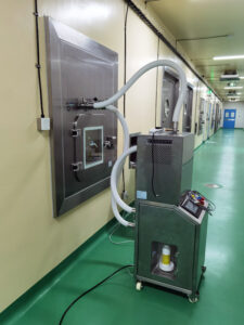
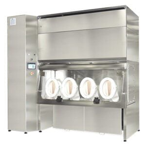
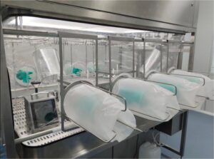
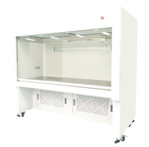
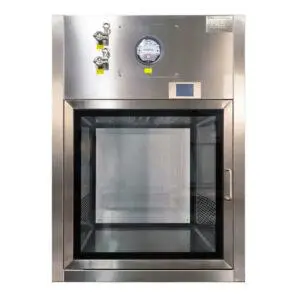
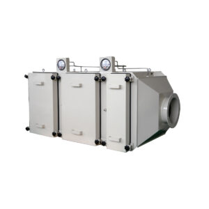
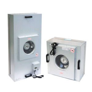
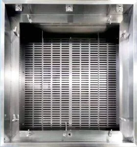
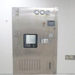
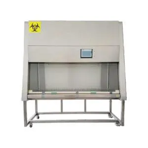
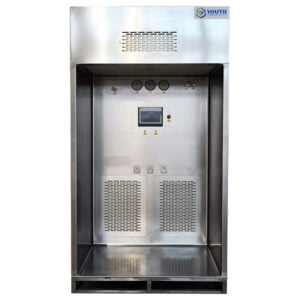
The foundation of any semiconductor cleanroom lies in its ability to maintain atmospheric purity at extraordinary levels. High-Efficiency Particulate Air (HEPA) and Ultra-Low Penetration Air (ULPA) filters form the backbone of contamination control, removing particles as small as 0.1 microns with 99.999% efficiency. Modern YOUTH Clean Tech filtration systems integrate multi-stage purification processes that address not only particulate matter but also molecular contamination and electrostatic discharge risks.
In our experience working with leading semiconductor facilities, the most critical factor isn’t just filter efficiency—it’s the uniformity of airflow distribution. Advanced cleanroom designs incorporate computational fluid dynamics modeling to ensure laminar flow patterns that eliminate dead zones where contaminants might accumulate. Temperature control systems maintain stability within ±0.1°C, while humidity management keeps relative humidity between 30-50% to prevent electrostatic buildup without encouraging microbial growth.
Wafer Processing and Handling Equipment
Semiconductor cleanroom equipment for wafer processing represents the most sophisticated manufacturing technology available today. Chemical vapor deposition (CVD) systems, plasma etching equipment, and ion implantation tools operate with precision measured in atomic layers. These systems must maintain vacuum levels of 10^-9 torr while controlling process temperatures to within single-digit variations.
| Equipment Type | Precision Level | Contamination Risk | Maintenance Frequency |
|---|---|---|---|
| CVD Systems | ±0.5 nm film thickness | Critical – molecular level | Weekly calibration |
| Plasma Etchers | ±2 nm etch uniformity | High – particle generation | Bi-weekly cleaning |
| Ion Implanters | ±1% dose uniformity | Moderate – sealed chamber | Monthly inspection |
| Wafer Handlers | ±10 micron placement | Critical – direct contact | Daily verification |
Contamination Monitoring and Detection Systems
Real-time particle counting systems provide continuous monitoring of cleanroom environments, detecting contamination events before they impact production. Laser-based particle counters can identify particles as small as 0.1 microns, while scanning electron microscopy enables detailed analysis of contamination sources. According to recent industry research, facilities using advanced monitoring systems reduce contamination-related yield losses by up to 40%.
Modern monitoring systems integrate artificial intelligence algorithms that learn normal operational patterns and flag anomalies before they escalate into production issues. These systems track not only particle counts but also chemical contamination, temperature fluctuations, and equipment performance metrics to provide comprehensive environmental oversight.
How Do Cleanroom Requirements Impact Semiconductor Manufacturing?
Classification Standards and Compliance
ISO 14644 standards define cleanroom classifications based on particle concentration limits, with Class 1 cleanrooms allowing no more than 10 particles per cubic meter of 0.1 micron or larger. Semiconductor manufacturing typically requires Class 1 or Class 10 environments, demanding specialized cleanroom equipment designed for extreme contamination control.
The transition from Class 100 to Class 1 cleanrooms has revolutionized semiconductor manufacturing capabilities. While Class 100 facilities enabled production of 200mm wafers with acceptable yields, today’s 300mm wafer processing and advanced node technologies below 7nm require the ultra-clean environment that only Class 1 cleanrooms can provide.
Process Integration Challenges
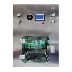
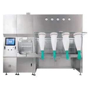
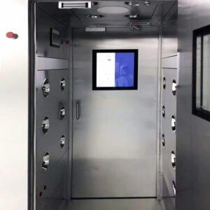
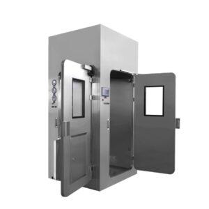
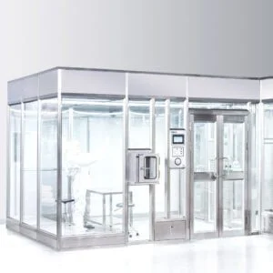
Integrating multiple process steps while maintaining cleanroom integrity presents significant engineering challenges. Each piece of equipment must not only perform its specific function but also contribute to overall contamination control. Equipment isolation protocols, transfer mechanisms, and inter-process storage systems must work seamlessly to prevent contamination introduction.
One major limitation of current cleanroom designs is the energy consumption required to maintain ultra-clean environments. Facilities typically consume 40-60% more energy than conventional manufacturing spaces, with air handling systems representing the largest energy draw. However, innovative equipment design increasingly focuses on energy recovery and optimization strategies.
Yield Impact and Economic Considerations
Cleanroom classification directly correlates with manufacturing yield, particularly for advanced semiconductor nodes. A single particle contamination event in a Class 10 environment might affect 5-10 wafers, while the same event in a Class 100 environment could impact 50-100 wafers. Industry data shows that upgrading from Class 100 to Class 1 environments typically improves yield by 8-15% for sub-10nm processes.
What Role Does Precision Manufacturing Equipment Play?
Measurement and Metrology Systems
Precision manufacturing equipment in semiconductor facilities includes advanced metrology tools that measure features smaller than the wavelength of visible light. Scanning electron microscopes, atomic force microscopes, and optical critical dimension measurement systems provide the dimensional accuracy required for nanometer-scale manufacturing.
As Dr. Maria Rodriguez from the International Semiconductor Manufacturing Consortium notes, “The metrology challenge grows exponentially as feature sizes shrink. We’re now measuring structures that are only a few atoms wide, requiring measurement precision that exceeds the stability of the equipment platform itself.”
Process Control and Automation
Modern semiconductor manufacturing relies heavily on automated process control systems that make real-time adjustments based on continuous monitoring data. These systems use statistical process control algorithms to maintain process parameters within extremely tight tolerances, often adjusting equipment settings hundreds of times per hour.
Equipment Synchronization and Workflow
The synchronization of multiple precision manufacturing systems requires sophisticated scheduling and control software. Equipment must coordinate not only process timing but also material handling, contamination control, and quality verification steps. Advanced facilities use AI-powered scheduling systems that optimize equipment utilization while maintaining quality standards.
How to Select the Right Semiconductor Processing Equipment?
Performance Specifications and Requirements
Equipment selection begins with a detailed analysis of process requirements, including throughput targets, precision specifications, and contamination control needs. Microelectronics cleanroom equipment must meet multiple criteria simultaneously: processing capability, contamination control, energy efficiency, and maintenance accessibility.
| Selection Criteria | Weight (%) | Key Metrics | Evaluation Method |
|---|---|---|---|
| Process Capability | 35% | Precision, throughput, repeatability | Benchmark testing |
| Contamination Control | 25% | Particle generation, outgassing rates | Environmental testing |
| Reliability | 20% | Mean time between failures, uptime | Historical data analysis |
| Total Cost of Ownership | 20% | Initial cost, operating expenses, maintenance | Financial modeling |
Integration and Compatibility Factors
Equipment compatibility extends beyond physical interfaces to include software integration, contamination control protocols, and maintenance scheduling. New equipment must integrate seamlessly with existing cleanroom infrastructure without compromising overall system performance.
Vendor Evaluation and Support
Vendor selection involves evaluating not only equipment performance but also technical support capabilities, spare parts availability, and upgrade paths. Leading semiconductor manufacturers typically maintain relationships with multiple equipment vendors to ensure supply chain resilience and competitive pricing.
What Are the Key Maintenance Strategies for Fab Cleanroom Equipment?
Preventive Maintenance Protocols
Fab cleanroom equipment requires sophisticated maintenance strategies that balance equipment availability with contamination control requirements. Preventive maintenance schedules must consider not only mechanical wear but also contamination accumulation, calibration drift, and component aging effects.
Contamination Prevention During Maintenance
Maintenance activities present significant contamination risks in cleanroom environments. Specialized procedures, tools, and materials are required to perform maintenance without compromising cleanroom integrity. Maintenance personnel must follow strict protocols including tool cleaning, material certification, and post-maintenance verification procedures.
Performance Optimization and Upgrades
Equipment performance optimization involves continuous monitoring of key performance indicators and systematic improvement of process parameters. Modern equipment includes built-in diagnostics and performance optimization algorithms that automatically adjust operating parameters to maintain optimal performance.
A recent case study from a leading Asian semiconductor manufacturer demonstrated how predictive maintenance reduced equipment downtime by 35% while improving process capability by 12%. The facility implemented AI-powered monitoring systems that predicted equipment failures 2-3 weeks before they occurred, enabling scheduled maintenance during planned production breaks.
Which Industries Benefit Most from Advanced Cleanroom Equipment?
Semiconductor and Microelectronics Manufacturing
The semiconductor industry remains the primary driver of cleanroom technology advancement, with facility investments often exceeding $10 billion for state-of-the-art fabrication plants. Advanced node production (7nm and below) requires the most sophisticated cleanroom equipment available, pushing the boundaries of contamination control technology.
Pharmaceutical and Biotechnology Applications
Pharmaceutical manufacturing increasingly adopts semiconductor-grade cleanroom standards, particularly for sterile drug production and biologics manufacturing. The precision and contamination control requirements for pharmaceutical applications often parallel those found in semiconductor manufacturing.
Aerospace and Defense Technologies
Aerospace component manufacturing, particularly for satellite and spacecraft applications, requires cleanroom environments to prevent contamination that could cause mission-critical failures. Military applications often demand even higher standards due to the extreme operating environments these components must withstand.
What Does the Future Hold for Semiconductor Cleanroom Technology?
Emerging Technologies and Innovations
The future of semiconductor cleanroom equipment focuses on several key areas: artificial intelligence integration, energy efficiency optimization, and modular design concepts. AI-powered contamination prediction systems are being developed that can forecast contamination events based on subtle environmental changes, enabling proactive intervention before issues impact production.
Industry Trends and Market Evolution
Market trends point toward increased automation, reduced human intervention, and enhanced monitoring capabilities. The integration of Internet of Things (IoT) sensors throughout cleanroom environments enables unprecedented visibility into environmental conditions and equipment performance.
Sustainability and Energy Efficiency
Environmental sustainability is becoming increasingly important in cleanroom design and operation. New equipment designs focus on energy recovery, reduced material consumption, and extended equipment lifecycles. Industry leaders are targeting 50% reduction in energy consumption per wafer produced over the next decade.
The semiconductor industry continues to push the boundaries of manufacturing precision, driving innovations that benefit numerous other industries. As feature sizes approach atomic scales and production volumes increase, the importance of advanced cleanroom equipment will only grow.
Looking ahead, the convergence of AI, advanced materials science, and nanotechnology will create new possibilities for contamination control and precision manufacturing. The next generation of cleanroom equipment will likely incorporate self-healing materials, quantum sensing technologies, and bio-inspired contamination control mechanisms.
For organizations seeking to implement or upgrade their cleanroom capabilities, the key lies in understanding that equipment selection is just the beginning. Success requires integrated thinking about processes, people, and technology working together to achieve unprecedented levels of precision and reliability. Consider exploring comprehensive cleanroom equipment solutions that can support your specific manufacturing requirements while positioning your facility for future technological advances.
Frequently Asked Questions
Q: What is a semiconductor cleanroom, and why is it essential in precision manufacturing?
A: A semiconductor cleanroom is a highly controlled environment designed to minimize contamination from dust, airborne microbes, and chemical vapors. This environment is crucial for precision manufacturing in the semiconductor industry because it ensures that delicate components and processes can be performed without defects, leading to higher yields and lower production costs.
Q: What are the key requirements for semiconductor cleanroom equipment?
A: Semiconductor cleanroom equipment must meet strict standards for maintaining a clean environment. This includes precise control over temperature, usually between 20°C and 22°C, and humidity levels to prevent environmental fluctuations. Additionally, air filtration systems such as HEPA or ULPA filters are used to remove particles, and the cleanroom’s air pressure is kept higher than outside to prevent contamination when doors are opened.
Q: How does semiconductor cleanroom equipment support various manufacturing processes?
A: Semiconductor cleanroom equipment supports critical processes like photolithography, etching, wafer processing, mask making, deposition, and cleaning. For instance, it ensures that wafers remain free from particles during processing, and masks used in photolithography are produced accurately without defects. Deposition processes also benefit from the clean environment, allowing for uniform and consistent material layering.
Q: What are the benefits of using semiconductor cleanroom equipment in precision manufacturing?
A: The use of semiconductor cleanroom equipment in precision manufacturing offers several benefits:
- Consistent Quality: It ensures that semiconductor devices are produced with consistent quality, reducing defects and improving yield.
- Cost Efficiency: By minimizing contamination and defects, production costs are lowered.
- Advanced Technology: Cleanrooms enable the manufacture of advanced semiconductor devices with tiny transistors and complex layers.
Q: How do industry standards influence the design and operation of semiconductor cleanrooms?
A: Semiconductor cleanrooms must comply with industry standards such as ISO 14644-1 and ISO 14644-2, which dictate cleanliness levels and quality control systems. These standards, along with other regulations from bodies like the EPA and SEMI Standards Program, ensure that cleanrooms operate under controlled conditions 24/7, maintaining the integrity of the manufacturing process.
Q: What role does air filtration play in semiconductor cleanroom equipment?
A: Air filtration is a critical component of semiconductor cleanroom equipment. It involves using high-efficiency filters like HEPA or ULPA to remove airborne particles, ensuring that the environment remains ultra-clean. This prevents particles from settling on wafers and devices during manufacturing, thereby reducing defects and improving product quality.
External Resources
Semiconductor Cleanrooms – Precision Environments – Details precision engineering and integration of turnkey semiconductor cleanroom equipment, emphasizing contamination control and bespoke manufacturing environments.
Role of Cleanroom Systems in the Semiconductor Industry | Fabtech – Explores the critical importance of cleanroom equipment and precision manufacturing technologies in semiconductor production, discussing industry standards and challenges.
Precision Cleanroom Products for Semiconductor Manufacturing | MISUMI – Offers customizable, precision-engineered cleanroom supplies and equipment for semiconductor manufacturing to ensure contamination-free environments.
Semiconductor Cleanrooms – A Comprehensive Overview – G-CON – Provides an in-depth overview of semiconductor cleanroom classifications, design principles, and environmental controls critical for precision manufacturing.
ISO Class 5 Semiconductor Cleanroom Fab – Precision Environments – Describes a completed ISO Class 5 modular semiconductor cleanroom project, including design, equipment, installation, and ongoing support for microelectronics manufacturing.
Precision Manufacturing and Cleanroom Equipment Overview | Terra Universal – Presents a range of precision cleanroom solutions, equipment, and modular components designed specifically for semiconductor manufacturing cleanroom environments.
Related Contents:
- Biotechnology Cleanroom Equipment | Sterile Processing
- Mobile LAF Carts for Semiconductor Industry: Guide
- Medical Device Cleanroom Equipment | ISO Class Requirements
- Cleanroom Equipment Types | Classification | Selection Guide
- Understanding Cleanroom Equipment Standards and Requirements
- Semiconductor Cleanroom HEPA Housing Box Specifications
- Modular Laminar Air Flow Units for Cleanrooms
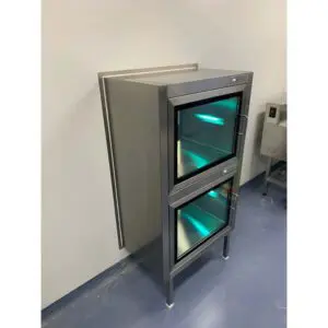
- LAF Garment Cabinets in Semiconductor Production
- How Often Should You Service Your LAF Unit? Expert Advice


