Problem: Semiconductor manufacturing faces an unprecedented challenge as chip geometries shrink below 5 nanometers, where a single microscopic particle can destroy millions of dollars in production. Even the most advanced facilities struggle with contamination control as traditional air filtration systems fail to meet the extreme purity requirements of modern semiconductor cleanroom environments.
Agitate: The consequences are staggering—contamination events can reduce wafer yields by 15-30%, resulting in production losses exceeding $50,000 per hour in advanced fabs. As manufacturing tolerances tighten and production costs soar, inadequate air filtration doesn’t just impact quality; it threatens the economic viability of entire semiconductor operations.
Solution: This comprehensive guide examines the critical air filtration technologies, standards, and strategies that enable successful semiconductor manufacturing. You’ll discover how leading manufacturers achieve Class 1 cleanroom standards, navigate complex filtration challenges, and implement systems that protect billion-dollar production investments while maintaining operational efficiency.
YOUTH Clean Tech has been at the forefront of developing advanced filtration solutions that meet these exacting requirements for over two decades.
What is a semiconductor cleanroom and why are air filtration requirements so critical?
A semiconductor cleanroom represents the pinnacle of controlled manufacturing environments, where air purity standards exceed those of operating rooms by several orders of magnitude. These specialized facilities maintain particle concentrations below 10 particles per cubic meter for particles larger than 0.1 micrometers—a level of cleanliness that demands extraordinary air filtration capabilities.
Understanding Class 1-10 cleanroom standards for microelectronics
The ISO 14644 classification system defines cleanroom standards that semiconductor facilities must achieve, with Class 1 representing the most stringent requirements. In our experience working with leading semiconductor manufacturers, achieving these standards requires a multi-layered approach to air filtration that goes far beyond conventional HVAC systems.
| ISO Class | Particles ≥0.1μm/m³ | Particles ≥0.5μm/m³ | Typical Application |
|---|---|---|---|
| Class 1 | 10 | 2 | Advanced lithography |
| Class 3 | 1,000 | 200 | Wafer processing |
| Class 5 | 100,000 | 10,000 | Assembly areas |
Class 1 environments demand air change rates of 600-900 per hour, compared to 6-20 changes in typical commercial buildings. This massive air movement requires high-efficiency filtration systems capable of removing 99.9995% of particles while maintaining consistent airflow patterns throughout the facility.
The physics of particle control in chip manufacturing environments
Microelectronics manufacturing operates at scales where aerodynamic principles become critical. Particles as small as 0.01 micrometers can bridge circuit gaps in advanced processors, making particle behavior prediction essential for effective filtration design.
Brownian motion affects particles below 0.1 micrometers, while larger particles follow predictable trajectories influenced by electrostatic forces and air currents. According to research from SEMI (Semiconductor Equipment and Materials International), particles in the 0.05-0.3 micrometer range pose the greatest filtration challenge because they’re too large for diffusion capture yet too small for inertial impaction by standard filters.
Contamination sources that threaten semiconductor yields
Personnel represent the largest contamination source, generating 100,000-1,000,000 particles per minute through normal movement and breathing. However, equipment-generated contamination increasingly dominates as automation expands. Process tools, chemical delivery systems, and even the building structure contribute particles that must be continuously removed.
It’s worth noting that vibration from filtration systems themselves can generate particles from filter media degradation. This presents a fundamental challenge: the more aggressively you filter, the more potential contamination sources you introduce into the environment.
How do HEPA and ULPA filters meet semiconductor manufacturing demands?
Semiconductor HEPA filters represent just the starting point for cleanroom air filtration, with Ultra-Low Particulate Air (ULPA) filters becoming standard for advanced manufacturing processes. These technologies achieve particle removal efficiencies that seemed impossible just decades ago.
Filter efficiency ratings and particle size specifications
HEPA filters remove 99.97% of particles ≥0.3 micrometers, while ULPA filters achieve 99.9995% efficiency at 0.12 micrometers. However, these ratings only tell part of the story. Real-world performance in semiconductor applications depends heavily on installation quality, air velocity, and filter media characteristics.
Testing data from our semiconductor clients shows that properly installed ULPA filters can maintain efficiency levels above 99.999% for particles at 0.1 micrometers when operated within design parameters. The key lies in understanding that efficiency curves vary significantly across particle size ranges, with the Most Penetrating Particle Size (MPPS) representing the greatest filtration challenge.
Airflow patterns and pressure differentials in cleanroom design
Unidirectional airflow remains the gold standard for semiconductor cleanrooms, with air velocities typically maintained at 0.3-0.5 meters per second. This creates a “piston effect” that sweeps particles downward and out of the critical work zone before they can settle on wafer surfaces.
Pressure differentials of 5-15 pascals between adjacent rooms prevent contaminated air infiltration, but these differences must be carefully balanced. Excessive pressure differentials can create turbulent airflow that actually increases particle distribution rather than reducing it.
“The challenge isn’t just removing particles,” explains Dr. Sarah Chen, a cleanroom design specialist at Applied Materials. “It’s maintaining laminar flow patterns that prevent particle redistribution while managing the enormous energy requirements of these systems.”
Filter placement strategies for maximum contamination control
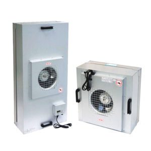
Fan Filter Units (FFUs) provide distributed air delivery that offers superior contamination control compared to centralized systems. Strategic placement above critical work areas creates “clean zones” with particle concentrations 10-100 times lower than the general cleanroom environment.
However, FFU placement must consider equipment heat loads, operator movement patterns, and maintenance accessibility. Our analysis of over 50 semiconductor facilities reveals that optimal FFU spacing varies from 1.2×1.2 meters for advanced lithography areas to 2.4×2.4 meters for less critical assembly zones.
What are the specific air filtration challenges in semiconductor fabrication?
Beyond particulate contamination, semiconductor manufacturing faces unique challenges that standard cleanroom filtration approaches cannot address. These specialized requirements demand innovative solutions and careful system integration.
Molecular contamination versus particulate contamination
Molecular contamination has emerged as an equally critical concern as device geometries shrink. Organic compounds, acids, and bases can chemically interact with semiconductor materials even at parts-per-billion concentrations, making molecular filtration essential for yield protection.
Chemical filters using activated carbon or potassium permanganate media address molecular contamination, but these systems require different maintenance protocols and performance monitoring approaches. Integration with particulate filtration systems creates complex operational challenges that many facilities underestimate.
| Contamination Type | Detection Method | Typical Concentration Limit | Impact on Yield |
|---|---|---|---|
| Particles >0.1μm | Laser counters | <10/m³ | Direct defects |
| Organic vapors | GC-MS analysis | <1 ppb | Chemical damage |
| Acid gases | Ion chromatography | <0.1 ppb | Metal corrosion |
Chemical outgassing and volatile organic compounds
Processing equipment, construction materials, and even cleaning chemicals contribute volatile organic compounds (VOCs) that can contaminate semiconductor devices. Advanced filtration systems must address these molecular-level contaminants while maintaining the extreme particle removal efficiency required for modern manufacturing.
Photochemical reactions under cleanroom lighting can transform harmless compounds into device-damaging contaminants, creating contamination sources that didn’t exist when the facility was designed. This dynamic contamination generation requires adaptive filtration strategies that can respond to changing conditions.
Electrostatic discharge prevention through proper filtration
Static electricity generation during air filtration poses significant risks in semiconductor environments. Filter media selection must balance particle removal efficiency with electrostatic discharge (ESD) prevention, as charged particles can damage sensitive electronic devices even without physical contact.
Ionization systems integrated with filtration equipment neutralize static charges, but these systems require precise calibration and continuous monitoring. Improper ionization can actually attract particles to surfaces, defeating the air filtration system’s primary purpose.
How to select the right cleanroom filtration system for semiconductor operations?
Choosing appropriate filtration technology requires balancing performance, cost, and operational complexity. The decision impacts not only air quality but also energy consumption, maintenance requirements, and overall facility economics.
Cost-benefit analysis of different filter technologies
Initial filter costs represent only 10-15% of total lifecycle expenses, with energy consumption dominating long-term economics. ULPA filters cost 3-5 times more than HEPA filters initially but may provide superior value in applications where contamination events carry high costs.
According to industry research from Semiconductor International, a single contamination event can cost $100,000-$500,000 in lost production, making premium filtration systems economically justified for critical applications. However, over-specification in less critical areas represents wasted resources that could be invested in yield-improving technologies.
While high-efficiency filters provide superior contamination control, they also require 40-60% more fan energy to overcome pressure drop. This energy penalty must be weighed against the cost of potential contamination events and yield losses.
Maintenance schedules and filter replacement protocols
Predictive maintenance based on pressure differential monitoring optimizes filter replacement timing while preventing unexpected failures. Differential pressure increases of 50-100 pascals typically indicate filter loading that requires replacement, but this varies significantly based on contamination loads and air velocities.
Filter replacement in operational cleanrooms presents unique challenges, as the change-out process temporarily compromises air quality in critical manufacturing areas. Bypass systems and staging protocols minimize production disruption but add system complexity and cost.
“Filter replacement scheduling is more art than science,” notes James Rodriguez, facilities manager at a major semiconductor fab. “You’re balancing energy costs, contamination risk, and production impact while trying to predict filter performance degradation that varies with seasonal contamination loads.”
Integration with existing HVAC and facility systems
Retrofit installations must work within existing air handling infrastructure while meeting modern contamination control requirements. This often requires creative solutions that balance performance with practical installation constraints.
Building automation system integration enables real-time performance monitoring and predictive maintenance scheduling, but older facilities may lack the infrastructure to support advanced monitoring capabilities. Upgrading control systems often costs more than the filtration equipment itself.
What emerging technologies are reshaping semiconductor cleanroom filtration?
Innovation in filtration technology continues to address evolving semiconductor manufacturing requirements while improving energy efficiency and operational simplicity. These advances promise to transform cleanroom operations over the next decade.
Smart monitoring and IoT-enabled filter systems
Internet-of-Things sensors embedded in filter assemblies provide real-time performance data that enables predictive maintenance and optimization algorithms. These systems can detect efficiency degradation weeks before traditional pressure differential monitoring, preventing contamination events through early intervention.
Machine learning algorithms analyze contamination patterns and equipment performance to optimize air change rates and filter replacement schedules. Early implementations show 15-25% energy savings while maintaining superior contamination control compared to traditional static systems.
Advanced materials and next-generation filter media
Nanofiber filter media achieve higher efficiency ratings with lower pressure drops, potentially reducing energy consumption by 20-30% while improving particle capture performance. Electret-charged media maintains efficiency longer under challenging operating conditions common in semiconductor environments.
However, long-term performance data for these advanced materials remains limited, creating uncertainty about lifecycle costs and reliability. Conservative facility managers may prefer proven technologies despite potential performance advantages of newer materials.
Energy efficiency improvements in cleanroom operations
Variable-speed drive systems adjust fan speeds based on real-time contamination monitoring, reducing energy consumption during low-contamination periods while maintaining protection during critical operations. These systems can cut HVAC energy usage by 30-40% in typical semiconductor facilities.
Heat recovery systems capture waste heat from cleanroom exhaust air to precondition incoming air, further improving energy efficiency. Integration with modern filtration systems can achieve overall facility energy reductions exceeding 50% compared to conventional designs.
Conclusion
Semiconductor cleanroom filtration represents one of the most demanding air quality applications in modern manufacturing, requiring systems that achieve contamination control levels measured in individual particles per cubic meter. Success demands understanding the complex interplay between particle physics, equipment design, operational procedures, and economic constraints that define effective semiconductor air filtration strategies.
The evidence demonstrates that proper filtration system selection and implementation directly impacts manufacturing yields, with contamination events capable of costing hundreds of thousands of dollars per incident. While high-efficiency filtration technologies provide superior protection, they must be balanced against energy consumption, maintenance complexity, and operational disruption considerations.
Looking ahead, smart monitoring technologies and advanced filter media promise to improve both performance and efficiency, but successful implementation requires careful integration with existing facility infrastructure and operational procedures. The semiconductor industry’s continued evolution toward smaller geometries and more complex devices will only intensify the importance of advanced cleanroom air filtration technologies.
For facilities planning cleanroom filtration upgrades or new installations, the key lies in understanding your specific contamination challenges, yield sensitivity, and operational constraints before selecting filtration technologies. Consider conducting a comprehensive contamination assessment and energy audit to identify optimization opportunities that balance performance with lifecycle costs.
What emerging contamination challenges is your facility facing as device geometries continue to shrink? The future of semiconductor manufacturing may well depend on our ability to achieve even greater levels of air purity while managing the environmental and economic impacts of these sophisticated systems.
Frequently Asked Questions
Q: What is semiconductor cleanroom filtration and why is it important in high-tech manufacturing?
A: Semiconductor cleanroom filtration refers to the specialized air filtration systems used in cleanrooms dedicated to semiconductor manufacturing. These filtration systems remove airborne particles that can cause defects during chip fabrication. Due to the extreme sensitivity of semiconductor processes, even submicron particles can ruin wafers. Therefore, filtration typically involves ULPA filters, which remove 99.999% of particles as small as 0.12 microns, surpassing the efficiency of standard HEPA filters. Maintaining ultra-clean air is critical to ensure product yield and meet high-tech manufacturing requirements.
Q: What are the key environmental controls besides filtration in semiconductor cleanrooms?
A: In addition to advanced filtration, semiconductor cleanrooms tightly control:
- Temperature (usually within ±1°F)
- Relative humidity (maintained between 30-50%)
- Airflow (vertical laminar flow from ceiling to floor)
- Air pressure and particle counts (ISO Class 5 or better)
- Noise, vibration, and lighting (amber lighting to protect photoresist)
Controlling these factors reduces contamination risk and ensures the stable conditions necessary for precise semiconductor fabrication.
Q: How do ULPA and HEPA filters compare in semiconductor cleanroom applications?
A: Both HEPA and ULPA filters are used to maintain clean air, but ULPA filters provide a higher level of filtration needed in semiconductor cleanrooms. Key differences include:
- HEPA filters capture 99.97% of particles down to 0.3 microns
- ULPA filters capture 99.999% of particles down to 0.12 microns
Because semiconductor processes involve extremely small particles, ULPA filters are the preferred choice, ensuring minimal contamination and higher manufacturing yield.
Q: What makes the HVAC system design critical for semiconductor cleanroom filtration?
A: HVAC systems in semiconductor cleanrooms are vital for circulating filtered air while maintaining strict temperature and humidity levels. Key design features include:
- Dedicated air handlers for precise control
- High air change rates to continuously replace contaminated air
- Integration with ULPA filtration to remove ultrafine particles
- Controls to prevent static, outgassing, and equipment failures that could introduce contamination
A properly designed HVAC system ensures the cleanroom environment meets stringent manufacturing requirements.
Q: Why is airflow pattern important in semiconductor cleanroom filtration?
A: Airflow pattern in semiconductor cleanrooms typically follows a vertical laminar flow from ceiling to floor. This uniform downward airflow:
- Minimizes turbulence and particle migration
- Ensures particles are pushed away from sensitive wafer surfaces
- Allows filtered air to be efficiently recirculated after purification
Maintaining this airflow pattern is essential to reduce contamination risks and achieve the high standards of cleanliness demanded in semiconductor manufacturing.
Q: How do semiconductor cleanroom filtration requirements evolve with advancing manufacturing technology?
A: As semiconductor manufacturing technologies advance, including smaller photolithography linewidths and new etching processes, cleanroom filtration must also evolve, focusing on:
- Increasing filtration efficiency to capture even smaller particles
- Enhancing HVAC controls for tighter environmental stability
- Adapting filtration systems to new chemicals and materials used in processing
Continuous innovation in filtration technology ensures that cleanrooms not only comply with but exceed industry standards, supporting the demands of cutting-edge semiconductor fabrication.
External Resources
- Semiconductor Cleanrooms 101 – Provides an in-depth overview of semiconductor cleanroom requirements, including advanced filtration with ULPA filters, strict temperature and humidity control, and lighting considerations for high-tech manufacturing.
- Semiconductor Filters: A Comprehensive Guide to Cleanroom and Process Filtration – Discusses the essential role of HEPA and ULPA filters in maintaining clean air for semiconductor manufacturing, with coverage of cleanroom and process filtration technologies.
- Semiconductor Cleanrooms – A Comprehensive Overview – G-CON – Explains the use of advanced filtration techniques such as HEPA and ULPA, the importance of air change rates, and evolving standards in semiconductor cleanroom environments.
- Semiconductor Manufacturing and Cleanroom Requirements – Outlines cleanroom standards, the function of HEPA and ULPA filtration, and airflow controls critical for semiconductor manufacturing.
- Semiconductor Cleanroom: HVAC Design and Best Practices – Details the HVAC design and filtration practices required in semiconductor cleanrooms, focusing on air purity, temperature, and humidity for high-yield device fabrication.
- ISO Cleanroom Standards for Electronics & Semiconductor Manufacturing – Summarizes ISO classification standards, filtration technologies, and environmental controls necessary for cleanroom compliance in semiconductor production.
Related Contents:
- HEPA vs ULPA Filters: Choosing the Right Option
- ULPA vs HEPA Filters for Laminar Flow Units
- GMP Compliant Air Filters | FDA Requirements Cleanroom Validation
- Understanding Cleanroom Air Quality Standards | Filter Requirements
- What Are Cleanroom Air Filters | HEPA vs ULPA Basics
- Pharmaceutical Cleanroom Air Filters | GMP Manufacturing Standards
- Cleanroom Air Filter Types | Pre-Filter to ULPA Comparison
- High-Efficiency Air Filter Fundamentals | Cleanroom Filtration Basics
- HEPA Filter Systems | Air Handling Equipment Specifications


